©Copyright 2019 SIKO POLYMERS (SUZHOU) CO., LTD All rights reserved.Site Map Powered by iwonder.cn

- Email Uskevin@sikopolymers.com

English


Clean and durable, PEEK is making its mark in semiconductors
As the COVID-19 pandemic continues and demand for chips continues to rise in sectors ranging from communications equipment to consumer electronics to automobiles, the global shortage of chips is intensifying.
Chip is an important basic part of information technology industry, but also a key industry affecting the whole high-tech field.

Making a single chip is a complex process that involves thousands of steps, and each stage of the process is fraught with difficulties, including extreme temperatures, exposure to highly invasive chemicals, and extreme cleanliness requirements. Plastics play an important role in semiconductor manufacturing process, antistatic plastics, PP, ABS, PC, PPS, fluorine materials, PEEK and other plastics are widely used in semiconductor manufacturing process. Today we'll take a look at some of the applications PEEK has in semiconductors.
Chemical mechanical grinding (CMP) is an important stage of semiconductor manufacturing process, which requires strict process control, strict regulation of surface shape and surface of high quality. The development trend of miniaturization further puts forward higher requirements for process performance, so the performance requirements of CMP fixed ring are becoming higher and higher.

The CMP ring is used to hold the wafer in place during the grinding process. The material selected should avoid scratches and contamination on the wafer surface. It is usually made of standard PPS.
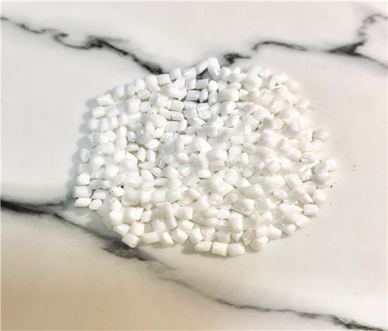
PEEK features high dimensional stability, ease of processing, good mechanical properties, chemical resistance, and good wear resistance. Compared to PPS ring, THE CMP fixed ring made of PEEK has greater wear resistance and double service life, thus reducing downtime and improving wafer productivity.
Wafer manufacturing is a complex and demanding process that requires the use of vehicles to protect, transport, and store wafers, such as front open wafer transfer boxes (FOUPs) and wafer baskets. Semiconductor carriers are divided into general transmission processes and acid and base processes. Temperature changes during heating and cooling processes and chemical treatment processes can cause changes in the size of the wafer carriers, resulting in chip scratches or cracking.

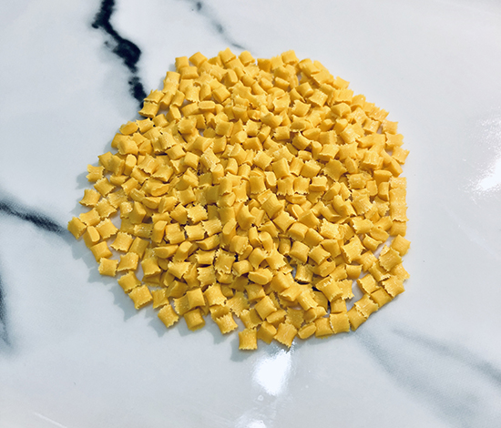
PEEK can be used to make vehicles for general transmission processes. The anti-static PEEK (PEEK ESD) is commonly used. PEEK ESD has many excellent properties, including wear resistance, chemical resistance, dimensional stability, antistatic property and low degas, which help prevent particle contamination and improve the reliability of wafer handling, storage and transfer. Improve the performance stability of front open wafer transfer box (FOUP) and flower basket.
Holistic mask box
Lithography process used for graphical mask must be kept clean, adhere to light cover any dust or scratches in projection imaging quality degradation, therefore, mask, whether in manufacturing, processing, shipping, transportation, storage process, all need to avoid contamination of mask and particle impact due to the collision and friction mask cleanliness. As the semiconductor industry begins to introduce extreme ultraviolet light (EUV) shading technology, the requirement to keep EUV masks free of defects is higher than ever.

PEEK ESD discharge with high hardness, little particles, high cleanliness, antistatic, chemical corrosion resistance, wear resistance, hydrolysis resistance, excellent dielectric strength and excellent resistance to radiation performance features, in the process of production, transmission and processing mask, can make the mask sheet stored in low degassing and low ionic contamination of environment.
Chip test
PEEK features excellent high temperature resistance, dimensional stability, low gas release, low particle shedding, chemical corrosion resistance, and easy machining, and can be used for chip testing, including high temperature matrix plates, test slots, flexible circuit boards, prefiring test tanks, and connectors.

In addition, with the increase of environmental awareness of energy conservation, emission reduction and plastic pollution reduction, the semiconductor industry advocates green manufacturing, especially the chip market demand is strong, and chip production needs wafer boxes and other components demand is huge, the environmental impact can not be underestimated. Therefore, the semiconductor industry cleans and recycles wafer boxes to reduce the waste of resources. PEEK has minimal performance loss after repeated heating and is 100% recyclable.